In recent years, as China has increased the transformation and upgrading of its manufacturing industry, major industrial manufacturers have begun to improve product quality for development. Among them, the PCB printed circuit board is the motherboard or substrate of electronic and electrical components. Any small device on the PCB may cause some function failure or even scrap the whole board. In addition, the competition of PCB manufacturing is becoming more and more fierce, and the quality requirements of users are also improving. Therefore, every node of PCB PCB from design to quality inspection needs strict quality control, and on-site inspection of PCB is required at any time.
PCB on-site inspection is the inevitable choice of manufacturers. At present, the manufacturing industry has higher and higher requirements for PCB quality. The whole process of PCB design, feeding, production and quality inspection needs strict quality control. In the actual production process of PCB, although it is not guaranteed that the product can reach 100% of the qualified rate, the defective rate of the product can be minimized and controlled within a reasonable range through effective quality detection and control measures.
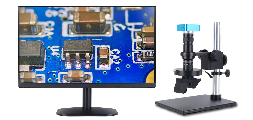
Video microscope is a powerful tool in PCB quality inspection. Because of its advantages of simplicity, portability, multi-function, and good image quality, it has become a sharp tool for electronic engineers to conduct on-site inspection, help them find various quality problems of PCB boards faster, find out the causes, and better control the quality of PCB boards.
Substrate: shallow pits on the surface or white spots, white spots, cavities or foreign matters on the inner layer; The size of the pressing plate changes or bends, warps, collapses or breaks; There are pits, pits, glue spots, creases or cracks on the surface of copper foil.
Hole location: drilling error, position deviation, hole blockage, hole type error, hole diameter distortion, hole wall roughness, hole wall dirt or too much attached debris, hole wall glass fiber protrusion, hole edge copper layer and base material peeling, etc.
Welding: false welding, continuous welding, missing welding, solder spatter, solder tip, foreign matter at solder joint, uneven ink, ink separation, finger print, etc.
Electroplating: uneven copper plating, insufficient copper thickness, drag shadow, copper leakage, holes, etc.
Text: such as displacement, uneven color, rough edges, moire, hyphenation, blurred printing, etc.
To sum up, in the whole production process of PCB, we can use video microscope to carry out detailed microscopic quality inspection of the above quality problems, which lays a good foundation for better finding the causes of PCB quality problems, mastering the overall quality situation, taking countermeasures, improving enterprise management efficiency, and increasing the market competitiveness of products.
Prev:None
Next:None
Copyright © 2016 深圳市微申时代科技有限公司. All Rights Reserved.